Volta-Based Tesla V100 Data Center GPU Shatters Barrier of 120 Teraflops of Deep Learning

NVIDIA today launched Volta™ — the world’s most powerful GPU computing architecture, created to drive the next wave of advancement in artificial intelligence and high performance computing.
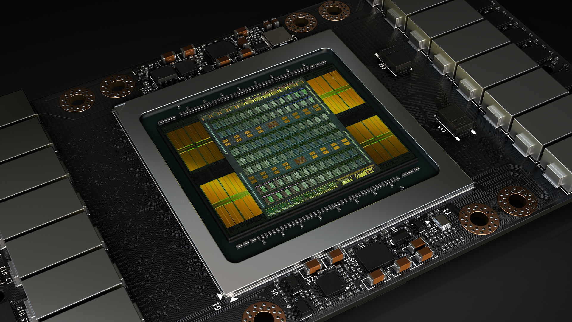
The company also announced its first Volta-based processor, the NVIDIA® Tesla® V100 data center GPU, which brings extraordinary speed and scalability for AI inferencing and training, as well as for accelerating HPC and graphics workloads.
“Artificial intelligence is driving the greatest technology advances in human history,” said Jensen Huang, founder and chief executive officer of NVIDIA, who unveiled Volta at his GTC keynote. “It will automate intelligence and spur a wave of social progress unmatched since the industrial revolution.
“Deep learning, a groundbreaking AI approach that creates computer software that learns, has insatiable demand for processing power. Thousands of NVIDIA engineers spent over three years crafting Volta to help meet this need, enabling the industry to realize AI’s life-changing potential,” he said.
Volta, NVIDIA’s seventh-generation GPU architecture, is built with 21 billion transistors and delivers the equivalent performance of 100 CPUs for deep learning.
It provides a 5x improvement over Pascal™, the current-generation NVIDIA GPU architecture, in peak teraflops, and 15x over the Maxwell™ architecture, launched two years ago. This performance surpasses by 4x the improvements that Moore’s law would have predicted.
Demand for accelerating AI has never been greater. Developers, data scientists and researchers increasingly rely on neural networks to power their next advances in fighting cancer, making transportation safer with self-driving vehicles, providing new intelligent customer experiences and more.
Data centers need to deliver exponentially greater processing power as these networks become more complex. And they need to efficiently scale to support the rapid adoption of highly accurate AI-based services, such as natural language virtual assistants, and personalized search and recommendation systems.
Volta will become the new standard for high performance computing. It offers a platform for HPC systems to excel at both computational science and data science for discovering insights. By pairing CUDA® cores and the new Volta Tensor Core within a unified architecture, a single server with Tesla V100 GPUs can replace hundreds of commodity CPUs for traditional HPC.
Breakthrough Technologies
The Tesla V100 GPU leapfrogs previous generations of NVIDIA GPUs with groundbreaking technologies that enable it to shatter the 100 teraflops barrier of deep learning performance. They include:
- Tensor Cores designed to speed AI workloads. Equipped with 640 Tensor Cores, V100 delivers 120 teraflops of deep learning performance, equivalent to the performance of 100 CPUs.
- New GPU architecture with over 21 billion transistors. It pairs CUDA cores and Tensor Cores within a unified architecture, providing the performance of an AI supercomputer in a single GPU.
- NVLink™ provides the next generation of high-speed interconnect linking GPUs, and GPUs to CPUs, with up to 2x the throughput of the prior generation NVLink.
- 900 GB/sec HBM2 DRAM, developed in collaboration with Samsung, achieves 50 percent more memory bandwidth than previous generation GPUs, essential to support the extraordinary computing throughput of Volta.
- Volta-optimized software, including CUDA, cuDNN and TensorRT™ software, which leading frameworks and applications can easily tap into to accelerate AI and research.
| Tesla Product | Tesla K40 | Tesla M40 | Tesla P100 | Tesla V100 |
|---|---|---|---|---|
| GPU | GK110 (Kepler) | GM200 (Maxwell) | GP100 (Pascal) | GV100 (Volta) |
| SMs | 15 | 24 | 56 | 80 |
| TPCs | 15 | 24 | 28 | 40 |
| FP32 Cores / SM | 192 | 128 | 64 | 64 |
| FP32 Cores / GPU | 2880 | 3072 | 3584 | 5120 |
| FP64 Cores / SM | 64 | 4 | 32 | 32 |
| FP64 Cores / GPU | 960 | 96 | 1792 | 2560 |
| Tensor Cores / SM | n/a | n/a | n/a | 8 |
| Tensor Cores / GPU | n/a | n/a | n/a | 640 |
| GPU Boost Clock | 810/875 MHz | 1114 MHz | 1480 MHz | 1455 MHz |
| Peak FP32 TFLOP/s | 5.04 | 6.8 | 10.6 | 15 |
| Peak FP64 TFLOP/s | 1.68 | 2.1 | 5.3 | 7.5 |
| Peak Tensor Core TFLOP/s | n/a | n/a | n/a | 120 |
| Texture Units | 240 | 192 | 224 | 320 |
| Memory Interface | 384-bit GDDR5 | 384-bit GDDR5 | 4096-bit HBM2 | 4096-bit HBM2 |
| Memory Size | Up to 12 GB | Up to 24 GB | 16 GB | 16 GB |
| L2 Cache Size | 1536 KB | 3072 KB | 4096 KB | 6144 KB |
| Shared Memory Size / SM | 16 KB/32 KB/48 KB | 96 KB | 64 KB | Configurable up to 96 KB |
| Register File Size / SM | 256 KB | 256 KB | 256 KB | 256KB |
| Register File Size / GPU | 3840 KB | 6144 KB | 14336 KB | 20480 KB |
| TDP | 235 Watts | 250 Watts | 300 Watts | 300 Watts |
| Transistors | 7.1 billion | 8 billion | 15.3 billion | 21.1 billion |
| GPU Die Size | 551 mm² | 601 mm² | 610 mm² | 815 mm² |
| Manufacturing Process | 28 nm | 28 nm | 16 nm FinFET+ | 12 nm FFN |


